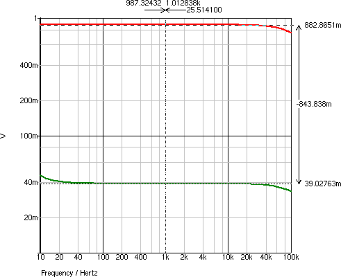
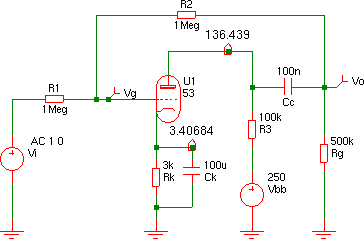
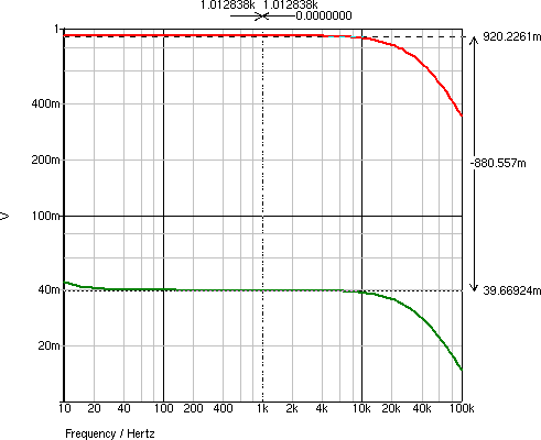
Vo と Vg の周波数特性は,図4のようになり,
ゲインは0.8829となります.
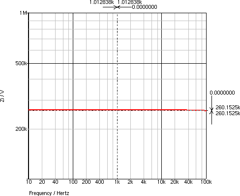
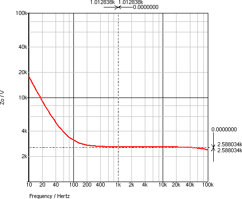
入力インピーダンスの周波数特性は,図5のようになり, Zi = 260.2 kΩ となります. 出力インピーダンスの周波数特性は,図6のようになり, Zo = 2.588 kΩ となります.
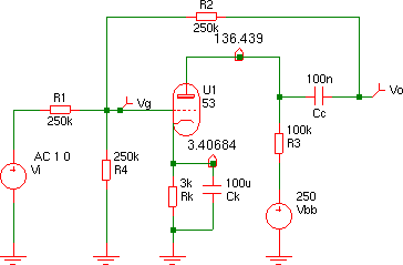
この回路の動作条件および三定数は,
| Ep0 | 133.0312 V | = | ||||||||
| Eg0 | -3.406857 V | = | ||||||||
| Ip0 | 1.135619 mA | = |
| x | = | 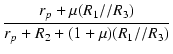 |
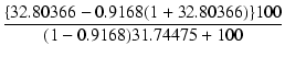
|
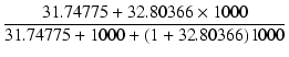
| = |  = 0.9168 = 0.9168 |
||
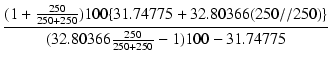
| A | = | -  . . 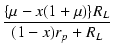 |
|
| = | -  . .  = - 0.8829 = - 0.8829 |
||
| x * | = | 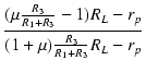 |
|
| = | 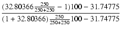 = 0.90955 = 0.90955 |
||
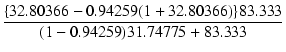
| R2 * | = | 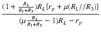 - (R1//R3) - (R1//R3) |
|
| = |  - (250//250) - (250//250) |
||
| = | 285.9 [kΩ] | ||
| Zi | = | 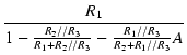 |
|
| = | 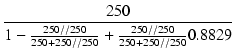 = 260.2 [kΩ] = 260.2 [kΩ] |
||
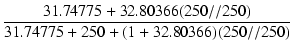
| Zo | = | (R2 + R1//R3)//RL// |
|
| = | (250 + 125)//100//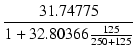 = 2.573 [kΩ] = 2.573 [kΩ] |
Vo と Vg の周波数特性は,図8のようになり,
ゲインは0.9202となります.
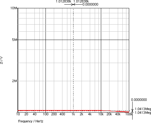
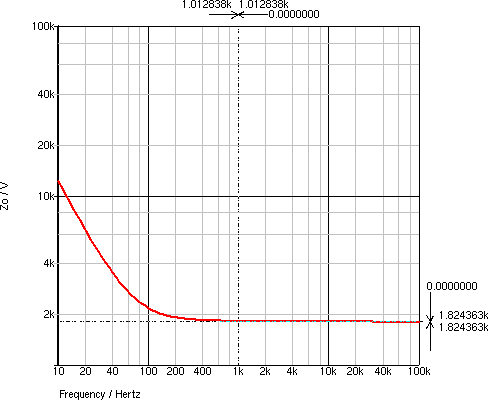
入力インピーダンスの周波数特性は,図9のようになり, Zi = 1041 kΩ となります. 出力インピーダンスの周波数特性は,図10のようになり, Zo = 1.824 kΩ となります. RL = Rp//Rg = 100//500 = 83.333 kΩ です.
| x | = | 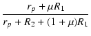 |
|
| = |  = 0.94259 = 0.94259 |
||
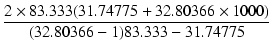
| A | = | - |
|
| = | -  = - 0.9206 = - 0.9206 |
||
| R2 * | = | 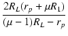 - R1 - R1 |
|
| = |  -1000 = 1090 [kΩ] -1000 = 1090 [kΩ] |
||
| Zi | = |  = =  = 1041 [kΩ] = 1041 [kΩ] |
|
| Zo | = | (R1 + R2)//RL// |
|
| = | (1000 + 1000)//83.333// = 1.783 [kΩ] = 1.783 [kΩ] |